Company address: No.2, West Pingbu Avenue, Huadu District, Guangzhou, Guangdong Province


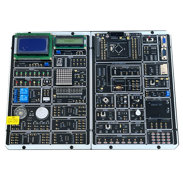
1、 Introduction and configuration instructions for each port of the core board
1) JTAG interface, used for connecting simulator interfaces such as ST LINKV2 and JINK;
2) USB/serial communication selection. The J2 jumper pin is inserted at the left end (U+to D+, U - to D -) for USB communication, while the J2 jumper pin is inserted at the right end (D+to R+, D - to R -) for RS232 serial communication;
3) J3: Start mode selection, when serial port burning, J6 jump pin is inserted in the (BOOT0-3.3V) position; During normal operation, the J6 jump pin is inserted in the (GND-BOOT0) position;
4) PAL, PAH, PBL, PBH, PDL, PDH, PEL, PEH: All IO ports are led out in an 8-core row; PA and PB all 32
Multiple IO ports are individually led out using 1mm gold holes, making it convenient for users to use.
(1) JP1, JP2 interfaces: used for the corresponding connection between the STM32 core board and the bottom plate of the experimental box.
(2) RST reset button. After the program download is completed, you need to press the reset button once to run the program.